OSE 3D Printed Circuits
Jump to navigation
Jump to search
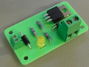
Concept: a 3D printed board serves as a structure for holding components so they are easy to solder. This can be described as dead-bug soldering with support structures. Note that Dead-Bug Soldering is useful for high frequency circuits - by the way.
- 3D print a circuit board with channels and physical infrastructure for holding all components.
- Bend the leads so they touch, and use wires to solder as needed. For through-hole components, this is fine.
- This is not fine for small feature advanced microelectronics, but 2.54 mm components would work.
- Soldering is quick for 2 wire components that touch each other. We can have the 3D print serve as a holding structure that makes soldering easy.
- 2nd option: wires snap in place if printed from elastomer. Ga 10 or 8 solid copper - just snap it in. Locking, snap-in Circuit cover finishes circuit. Components become 100% reusable!
- 3rd connection option: Not also - if 2 leads are inserted into a hole, the hole can be plugged with a solid copper conductor for good contact.
- Terminal blocks can be 3d printed in place!
- Note that we can make connectable modules with this technique, where 3D circuit blocks can plug into one another.
Other ideas
- TEST using a dual extruder printer to place conductive fulfillment in a print.
- such as, but would want lower resistance than 100kohm... https://hobbyking.com/en_us/conduct-electricity-abs-3d-printer-filament.html?countrycode=US&gclid=CjwKCAjwwZrmBRA7EiwA4iMzBI_jQE3oiTDjLxUGxKI7EA9xk4DzdBZ3MGNXzdm0TRXLhxfncVG2HBoC0qgQAvD_BwE&gclsrc=aw.ds
- TEST: Conductive filament could be shaped in such a way as to achieve a spring like grabbing of electronic parts?
- TEST: Could other features be printed to push SMA or other topologies onto these printed pins? think of placing the parts and having pressure applied from a heatsink above to press onto these special "pins"
Pros:
- Full 3D, body-integrated circuits can be produced.
Cons:
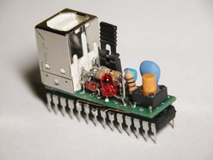
- Cons: limited to relatively large components - such as atmega328p DIP. But socketing can extend range of applicability, such as SOIC to SMT [1]
(Not OSE circuits. See Dead-Bug_Soldering, Circuits on Plastic, and Snap Together 3D Printed Electronics Modules for source.)
OSE Relevance
- In upcoming Incentive Challenge - we can require structure integrated circuits that are 3D printed in 3D, and fully recyclable!


