OSE 3D Printed Circuits: Difference between revisions
Jump to navigation
Jump to search
No edit summary |
No edit summary |
||
| Line 8: | Line 8: | ||
[[File:plasticcircuit.png|300px]][[File:deadbugarduino.jpg|300px]] | [[File:plasticcircuit.png|300px]][[File:deadbugarduino.jpg|300px]] | ||
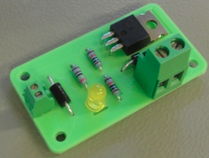
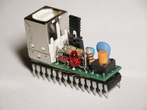
(Not OSE circuits. See [[Dead-Bug_Soldering]] and [[Circuits on Plastic]] for source. | |||
Revision as of 20:33, 28 April 2019
Concept: a 3D printed board serves as a structure for holding components so they are easy to solder. This can be described as dead-bug soldering with support structures. Note that Dead-Bug Soldering is useful for high frequency circuits - by the way.
- 3D print a circuit board with channels and physical infrastructure for holding all components.
- Bend the leads so they touch, and use wires to solder as needed. For through-hole components, this is fine.
- This is not fine for small feature advanced microelectronics, but 2.54 mm components would work.
- Soldering is quick for 2 wire components that touch each other. We can have the 3D print serve as a holding structure that makes soldering easy.

 (Not OSE circuits. See Dead-Bug_Soldering and Circuits on Plastic for source.