Adjustable Power Supply v18.08: Difference between revisions
m (→Main Circuit) |
|||
| Line 146: | Line 146: | ||
===Buck-Boost Converter=== | ===Buck-Boost Converter=== | ||
=====Main Circuit===== | =====Main Circuit===== | ||
Switching Transistors: [https://www.digikey.ca/short/jnjmwq MOSFET N-CH 60V 100A POWERDI5060] or [https://www.digikey.ca/short/jnjmwh MOSFET N-CH 60V 200A TO-220-3] | Switching Transistors: [https://www.digikey.ca/short/jnjmwq MOSFET N-CH 60V 100A POWERDI5060] or [https://www.digikey.ca/short/jnjmwh MOSFET N-CH 60V 200A TO-220-3] | ||
| Line 154: | Line 152: | ||
Rectifier Diode: [https://www.digikey.com/short/jwt9dh DIODE SCHOTTKY 250V 40A TO220AB] | Rectifier Diode: [https://www.digikey.com/short/jwt9dh DIODE SCHOTTKY 250V 40A TO220AB] | ||
PWM Controller: [https://www.digikey.com/short/jnjwcd IC REG CTRLR BUCK/BST 20HTSSOP-B] | PWM Controller: [https://www.digikey.com/short/jnjwcd IC REG CTRLR BUCK/BST 20HTSSOP-B] or [https://www.digikey.com/short/pc3rrv IC REG CTRLR BUCK-BOOST 20QFN] or 555 Timer | ||
555 Timer: [https://www.digikey.com/short/pc3r5z IC OSC SINGLE TIMER 3MHZ 8-SOIC] | |||
Digital Potentiometer: [https://www.digikey.com/short/j0rqqt IC DGTL POT 10BIT 16TQFN], 50 kOhm resistor | Digital Potentiometer: [https://www.digikey.com/short/j0rqqt IC DGTL POT 10BIT 16TQFN], 50 kOhm resistor | ||
Revision as of 00:26, 17 December 2018
In Progress
Arduino code for voltage sensing and control
Arduino code is hosted here. This code is far from finalized and represent only one of many possible design approaches. Post as many variations or improvements as you can as long as they have advantages.
Next steps: - implement I2C to control digital potentiometer
Design buck/boost converter module
For affordable buck-boost that can change voltage by a factor of five, high frequencies are needed to reduce inductor size. The Arduino has a limited PWM frequency (less than 100 kHz?). It may be possible to use a high-frequency buck-boost controller IC to handle the PWM, and control it with the Arduino via a digital potentiometer.
Volt-second balance on the inductor means that the average voltage across it over one switching cycle is zero
Discontinuous mode is when current through the output inductor is zero for part of the switching cycle
Next steps: - simulate main circuit - figure out how to switch between buck and boost configuration or simplify configuration - make bill of materials for prototyping
Figure out ways to salvage or build transformers
Investigate ways to use high frequency for more efficiency in power transformation as well as smaller inductors.
With new Silicon Carbide MOSFET technology, maybe feasible to use flyback transformer at high frequency as described here.
A flyback transformer could more compact and cheaper initially, but the lifetime cost of replacing a large input capacitor would likely outweigh the initial savings. It is also more complex than an AC transformer, so probably not the best choice for this application.
Design
Applications
Powering 3D printer
Workbench power supply
Charging batteries
Requirements
At least 360W output (12V at 30A)
Adjustable DC voltage output up to 24V
120Vac input
Research
Existing Open-Source Projects
Programmable bench power supply EEZ H24005
General
Safety Considerations in Power Supply Design
Common collector amplifiers can be used as voltage buffers
How to Increase the Bandwidth of Digital Potentiometers 10x to 100x
Ripple Port to Reduce Output Capacitor Size
Isolation in Digital Power Supply
Fundamentals of Gate Driver Circuits
Open-source based synthetic medium-voltage grid model for distribution power supply systems
Current Sharing in Parallel Diodes
Voltage Conversion
This page is a great guide.
Understanding Buck-Boost Power Stages
Flyback Transformer
The Active Clamp Flyback Converter: A Design Whose Time Has Come
A Comparison of Different Snubbers for Flyback Converters
Inductor and Flyback Transformer Design
1200 WATT FLYBACK SWITCHING POWER SUPPLY WITH SILICON CARBIDE SEMICONDUCTORS
Inductor volt-second balance, capacitor charge balance, and the small ripple approximation
Flyback transformer design considerations for efficiency and EMI
PASSIVE LOSSLESS SNUBBERS FOR HIGH FREQUENCY PWM CONVERTERS (page 41)
Modules
Flyback Transformer
A flyback transformer would most likely be operated in continuous conduction mode, so transformer size will be limited by core saturation. A toroid with powder core could be a suitable solution.
Switching speeds of MOSFET and diodes should be minimized to reduce switching losses. Winding losses should be minimized as well.
Selecting a Distributed Air-Gap Powder Core for Flyback Transformers
Calculations
With only 30 kHz, a large and expensive inductor would be needed.
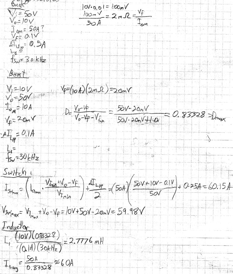
Buck-Boost Design Calculations
Digital potentiometer calculations
Conceptual Design
These designs may not be safe or functional. Use at your own risk.
KiCAD Symbol Generator, DB9851.lib, UC24612.lib
Buck-Boost Converter

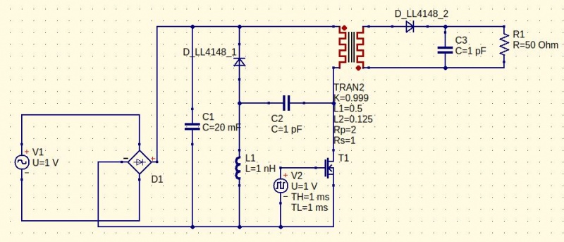
Flyback Configuration
https://wiki.opensourceecology.org/images/thumb/f/fc/FlybackDraft.jpg/800px-FlybackDraft.jpg edit
DRAFT, values are not correct
10 gauge wire for secondary winding. Primary has 8.5 turns, try 3 or 3.5 for secondary.
Software
Possible Parts
Output Capacitor: Aluminum (cheaper but more lossy), organic semiconductor (good overall), tantalum (best for surface mount) [1]
Output Inductor: Bobbin or rod-core cause more noise [2]
Isolator: DGTL ISO 2.5KV 2CH GEN PURP 8DIP
Synchronous Rectifier IC: SOT-23-5
Digital Potentiometer: IC DGTL POT 10BIT NV 14-TSSOP
Buck-Boost Converter
Main Circuit
Switching Transistors: MOSFET N-CH 60V 100A POWERDI5060 or MOSFET N-CH 60V 200A TO-220-3
Inductor: FIXED IND 33UH 30A 1.9MOHM SMD (would require 2.5 MHz switching frequency)
Rectifier Diode: DIODE SCHOTTKY 250V 40A TO220AB
PWM Controller: IC REG CTRLR BUCK/BST 20HTSSOP-B or IC REG CTRLR BUCK-BOOST 20QFN or 555 Timer
555 Timer: IC OSC SINGLE TIMER 3MHZ 8-SOIC
Digital Potentiometer: IC DGTL POT 10BIT 16TQFN, 50 kOhm resistor
Input/Output Capacitor: CAP CER 15UF 100V X7S SMD
PWM Control
High-side gate driver: IC HIGH-SIDE DVR HS HV 8-MSOP
Gate driver bootstrap diode: DIODE GEN PURP 100V 200MA SOD80
Oscillation setting: CAP CER 47PF 50V C0G/NP0 0201, 4.7 kOhm resistor
Short circuit protection timer: CAP CER 0.47UF 100V X7R 0805
Error Amp Feedback: CAP CER 0.068UF 100V X7R 0805, 100 Ohm resistor
Voltage Sensing
Voltage divider: RES SMD 442K OHM 1% 1/16W 0402, RES SMD 4.99M OHM 1% 1/16W 0402
Op amp for voltage buffer: IC OPAMP GP 1MHZ RRO SOT23-5
Control Circuit Power
Voltage regulator: IC REG BUCK 12V 1A TO220-5
Forward Configuration
Transformer: XFRMR TOROIDAL 500VA CHAS MOUNT, Investigating ways to salvage transformers
Rectifier: RECT BRIDGE FAST 3PHASE I4-PAC-5
IRFP250NPower transistor (MOSFET) driven by TC1411 1A High-Speed MOSFET Driver with pulse signal originating from arduino.
(Alternative mosfets requiring no mosfer driver) IRF540N "IR" MOSFET N-Channel 33A 100V IRFP250N
Switching Transistor: MOSFET N-CH 40V 95A TO-220AB
Flyback Configuration
Cost of components ~$80
Fuse: FUSE GLASS 15A 250VAC 5X20MM
Bridge Rectifier: 50A, 600V BRIDGE RECTIFIER, GBJ, DIODE BRIDGE FAST DIODE ECO-PAC1, 50A, 1000V BRIDGE RECTIFIER, GBJ
Input Capacitor: CAP ALUM 18000UF 20% 160V SCREW
Snubber
Snubber Diode: DIODE SCHOTTKY 250V 40A TO220AB
Snubber Capacitor: CAP CER 0.18UF 250V X7R 1812
Active Snubber Control: Active clamp flyback controller UCC28780D
Gate Driver Transistors: TRANS NPN 60V 3A TP, TRANS PNP 60V 5A TO-126
Integrated Gate Driver: IC DRIVER HI/LO SIDE 600V 14-DIP
Coupled Inductor
Switching Transistor: MOSFET NCH 650V 21A TO247N, MOSFET NCH 650V 39A TO247N
Transformer: FIXED IND 10UH 16.9A 5.1 MOHM TH, Kool Mu 77130A7 (11.2mm outer diameter, permeability = 125 u)
Output Rectifier
Output Diode: DIODE SCHOTTKY 45V 60A TO247AD
Synchronous Rectifier IC: SYNC RECTIFIER FLYBACK
Synchronous Rectifier Transistor: MOSFET N-CH 40V 95A TO-220AB