Circuits on Plastic: Difference between revisions
Jump to navigation
Jump to search
No edit summary |
No edit summary |
||
| Line 1: | Line 1: | ||
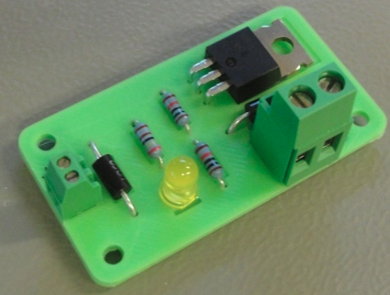
Example from [https://www.youmagine.com/designs/ultimaker-heated-bed-mosfet-relay-hack-v2#!design-information]. But, the back is awkward - for production-grade circuits, detailed channels and structures should be printed on the back to facilitate wire routing and soldering | Example from [https://www.youmagine.com/designs/ultimaker-heated-bed-mosfet-relay-hack-v2#!design-information]. But, the back is awkward - for production-grade circuits, detailed channels and structures should be printed on the back to facilitate wire routing and soldering. Note that in this example, the screw terminal coudl be 3d printed as well! | ||
[[File:plasticcircuit.png]] | [[File:plasticcircuit.png]] | ||
Revision as of 20:29, 28 April 2019
Example from [1]. But, the back is awkward - for production-grade circuits, detailed channels and structures should be printed on the back to facilitate wire routing and soldering. Note that in this example, the screw terminal coudl be 3d printed as well!
