Inverter

File:Step wave inverter concept.skp
Introduction
An open source inverter appears! In development.
Boost Converter
Notes: linear regulators may not be able to handle 72V input, so switching step-down regulator needed in between the 72V and linear regulators.
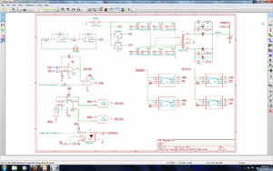
General Schematic
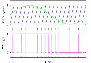
Control Waveform Diagram
In order to understand the control waveform diagram, the concepts "amplification", "sum (superposition)", and "comparator" must be understood.
Carrier Wave and Reference Wave, Combine and Transform! Transformers- waveforms in disguise.
The blue triangle wave is the carrier wave. High frequency.
The green sine wave is the reference wave. Desired output frequency and waveform.
The pink square wave is the PWM wave. It's what you get when you combine the carrier wave and the reference wave into a comparator. When the reference wave is a higher voltage than the carrier wave, the pink square wave is high voltage. When the reference wave is a lower voltage than the carrier wave, the pink square wave is low voltage.
Why do you want me to step the DC up?
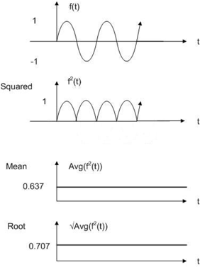
- Note, the squared graph is not entirely correct (e.g. (0.5)^2 = .25 not equal to .5), the curve descends steeper at first and then less and less, finally there is no kink in the curve. Sorry for that. (What we've depicted is |f(t)|, i.e. the absolute value (i.e.where f negative, |f| is positive)) see Mathematica.
What the hell is a root mean square?
Design Methodology
Outline of suggested design methodology (from Darren Vandervort, formerly of R&D of Power Electronics at Intel)
- The first step is to come up with design goals, and define constraints. (time, budget, power, size for example.)
- Pros and cons of different design paths are measured against goals and constraints, and a design path is chosen. (at this point the design goals are more or less locked. The design dictated which path was chosen, and if that changes the path will most likely change and any work performed after this point is wasted.)
- Schematic capture and part sourcing. These are inherently linked and lots of compromises are made during this step to match the values you described. For example, there may be a pre-manufactured module that can save time, but cost more money in the final design.
- Simulation and refinement. Simulation has become much more reliable in the last 6-7 years and this will save several iterations and the results are fed back into the schematic capture phase. After this phase is done the design should be considered closed. Simulation is great for exploring off-nominal behavior such as overload, low power factor, reverse power from load, etc.
- Layout. This is the design of the actual PCB. For high frequency there is an extra simulation step here as well because the layout becomes a much larger part of how the circuit performs. Unless one of the constraints for this design is "as small as possible" the frequencies involved will not necessitate simulation here.
- Prototype and testing. I would not consider the first design to be the first version. There are always things overlooked by the engineer that will have to be addressed.
Design Goals
Input: approx. 72VDC
Output: 120VAC 60Hz pure sine wave 5kW - 10kW
Design Paths
Step Down + Voltage Regulators: to 3.3V or 5V
Step Up + Voltage Regulators: to 170V
Digital Reference Sine Wave Generation
Carrier Wave Generation
PWM Driver
Power Handling: H Bridge with MOSFETs
Buck/Boost converter? Multi-tap Transformer?
Feedback: Error into PID Loop into amplitude factor of reference wave amplification
Schematic
Simulation
Layout
Printed Circuit Assembly
Case and External Connections
Complete Assembly
Old Notes
In summary, use a voltage regulator with circuitry to make a reference sine wave at the desired AC frequency and a carrier triangle wave at high frequency, compare the two waves to get a PWM signal and run that into an H-bridge with high DC input from a boost converter, then followed by a filter and a feedback circuit. Tada, inverter.
Industry & Open Source Research
Inverter Papers
Some from Universal Power Supply/Research Development.
- 100kW open source inverter for AC induction motor - [1]
- Paper on Low-Power Square Wave Inverter Including Circuit Diagram and Specific Explanations
- Paper on Medium Power True Sine Wave Inverter Including Circuit Diagram and Bill of Materials
- DC/AC Pure Sine Wave Inverter
- Solid Oxide Fuel Cell Inverter
- review of inverter use
Other DIY Inverters
- Arduino microinverter - [2]
- 1kW Michigan State U student capstone paper - [3]
- 10 kW induction heater + inverter circuit - [4]
- Microwave Transfomers - they propose to use modified transformers from old microwave ovens, you’d need about 10 broken micros’ and 20 N-type power MOSFET’s for a 9kw unit. [5]
- Open Source 100kW Electric Vehicle Controller/Inverter. This is a senior project for electrical vehicles. Its out is 3 phase. This could be of interest for the induction furnace. The design is very simple. Not sure if it was ever implemented. It is made mostly from IC's. Maybe these could be replaced to reduce some of the costs. [6]
- Solar Grid-Intertie Inverter - http://www.timnolan.com/index.php?page=solar-grid-intertie-inverter
- 500W Inverter - [7]
- Open Source Software and ARM based control board for driving an AC induction motor with V/Hz or FOC - tumanako.net
Scalable Commercial Inverter
The company MGE UPS seems to have merged with another one named APC, but the concept is good. This inverter is scalable up to 20kw. It looks like the inverters are designed to share some resources and are just connected in series.
(bad link) http://rep.mgeups.com/3ppdf/s4.pdf
From wikipedia on scalable 3 phase AC: To construct inverters with higher power ratings, two six-step three-phase inverters can be connected in parallel for a higher current rating or in series for a higher voltage rating. In either case, the output waveforms are phase shifted to obtain a 12-step waveform. If additional inverters are combined, an 18-step inverter is obtained with three inverters etc. Although inverters are usually combined for the purpose of achieving increased voltage or current ratings, the quality of the waveform is improved as well. 1
Arduino Based Inverters
- http://www.arduino.cc/cgi-bin/yabb2/YaBB.pl?num=1287161833
- http://www.kerrywong.com/2010/03/12/a-power-inverter-with-arduino-pulse-source/
Unevaluated Links from Gabrielle Leblanc
http://www.youtube.com/watch?v=aY9qmeA8gVI Homemade 1.8kW Inverter-Generator
http://www.youtube.com/watch?v=aLAXaB9t7GU Homemade Battery Charger & Generator
http://www.youtube.com/watch?v=GmZ5-9a0Rac&feature=plcp update to above
Legacy Inverter Designs
I2K Power Inverter
This is a decently well documented inverter system, 2 kW, using transformers. See: http://192.197.62.35/staff/mcsele/i2k.htm
- Disadvantages: about 70-80% efficient; appears that non-solid state inverters are less efficient than solid state. The author also confesses it is an older design, that uses a software generated PWM signal.
- Commercial, solid-state inverters are 90-95% efficient (ex., [8])
Institute for Appropriate Technology Inverter
Smaller-power, lightly documented example, up to 1000W: http://www.i4at.org/lib2/inverter.htm


